Evidence-first notes on bioscience and deep tech, at the edge of the lab and the market. Information only — not investment advice. Computing-power series, Part 3.
The 30-second version
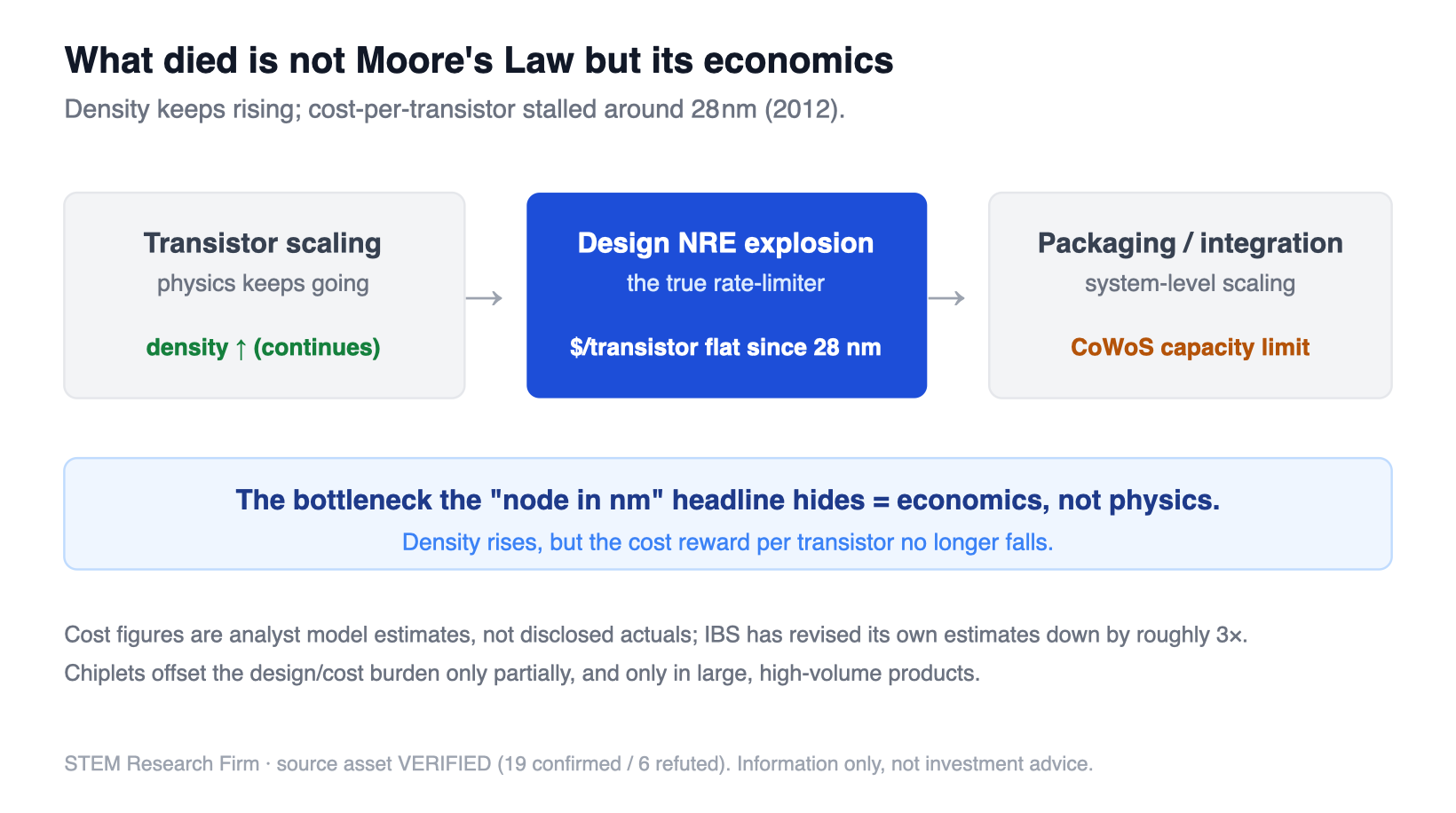
- What. The real bottleneck hidden behind the “node in nm” headline is not physics but economics — density keeps rising, but the decline in cost-per-transistor ($/transistor) stalled around 28nm (2012).
- So what. The compounding of rising wafer prices and exploding design NRE (non-recurring engineering) means the leading edge is affordable to only a few customers; chiplets offset this cost only partially, and only in large, high-volume products.
- Now what. Watch whether $/transistor resumes falling, the count of leading-edge tape-outs, and chiplet savings. Caveat: most cost figures below are analyst model estimates, not disclosed actuals. IBS has a track record of revising its own estimates down by roughly 3x, so the headline “only a few can afford it” figures may be overstated.
Series Part 3. The underlying knowledge asset passed 3-vote adversarial verification (VERIFIED — 19 confirmed / 6 refuted / 0 unverified, synthesis succeeded, 6 hype claims killed). Skeptic grade: proceed-with-caveats. For information only; not investment advice.
The five-minute read
Moore’s Law was an economic proposition, not a physical one
The essence of Moore’s Law was never “transistors keep shrinking” but the economic claim that cost-per-transistor halves every two years. The physics of scaling (GAA, backside power) still has a few nodes left. The problem is that this physical scaling is no longer “free.” Transistors still get smaller, but the economic bottleneck of cost-per-density that no longer falls stands right beside it.
Two facts confirmed by adversarial verification are the starting point. (a) Manufacturing cost rises faster than density gains (CONFIRMED). (b) But this is not “the first inflection point at N2” — it is a plateau accumulated since roughly 28nm / finFET (2012); the “first / first time” framing is REFUTED. The widely circulated “5nm inflection” / “first rise at 2nm” narrative rests only on wafer-price reporting (EETimes), with no measured $/transistor curve.
The true rate-limiter is wafer price x design cost, compounded
Leading-edge cost is the composite of three axes. Wafer price by consensus estimate is roughly TSMC N3/N3E ~$19,500, N5/N4 ~$18,500, N7 ~$9,500, 28nm ~$3,000 (TSMC does not disclose, so estimates vary by ±30%), and TSMC has signalled 5–10% annual increases on sub-5nm from 2026. Design NRE jumps from 28nm $30–50M to 5nm $200–400M to 3nm $400–600M+, and this is the true rate-limiting step behind the claim that “only hyperscalers, Apple and Nvidia can afford the leading edge.”
But here the Skeptic matters. The IBS headline of 5nm $542.2M is a modeling upper bound, not a measurement. IBS has a track record of revising its own estimates down by roughly 3x (applying the same discount gives an actual 5nm of ~$280M, about half the headline), so the “only a few can afford it” narrative may be overstated.
Chiplets are not a cure-all but a conditional offset
Chiplets cut die cost by up to ~50% versus monolithic (modeled), but packaging overhead (MCM ~25%, 2.5D ~50%) offsets a large share. A 5nm, 800mm² multi-chip design reaches payback only at around 2 million units, so for single, low-volume products monolithic is usually cheaper. The axis of economics shifts from scaling to packaging and integration (system-level scaling) — but packaging inherits its own bottleneck (CoWoS capacity).
Deep dive
1. Background — Moore’s Law as an economic proposition
Read Moore’s Law as physics (feature-size reduction) and the answer is “a few more nodes to go.” But the proposition that actually drove the industry was the economic claim that “cost-per-transistor halves every two years.” The inherited facts fixed by adversarial verification in this series’ Part 0 are the foundation: N2 wafer ~$30k, A16 rumored ~$45k, “manufacturing cost rises faster than density gains” CONFIRMED, but “first cost-per-transistor inflection” REFUTED (a cumulative trend since roughly 28nm / finFET, not a new event), plus the end of Dennard scaling and dark silicon. The series’ through-line is that “the bottleneck is elsewhere,” and in Part 3 that elsewhere is economics, not physics.
2. What this part newly established
The core is the separation of “density keeps rising” (fact) from “cost-per-density no longer falls” (economic bottleneck). Transistors keep shrinking, but the economic reward vanished around 2012.
- $/transistor has been flat since roughly 28nm (2012) — CONFIRMED (3-0). The historical 0.7x per-node cost reduction stopped at 28nm / finFET; normalized to 28nm, the cost of 100M transistors is flat to slightly rising at subsequent nodes. This is a 10-year accumulated plateau, not a new N2-driven inflection. Sources are Google’s Milind Shah (IEDM 2023), Or-Bach (2014) and IBS, mutually reinforcing. But this is a modeling / normalized metric (customer stakeholder charts), not an independent audit.
- “First rise / inflection at N3->N2” = narrative, not measurement — CONFIRMED (3-0). This framing rests only on wafer-price reporting (EETimes), has no measured or modeled $/transistor curve, and contradicts the 28nm plateau data. The “first time” phrasing exists only in EETimes and content-farm echoes.
3. Strengths and limits of the methodology
Strengths. The underlying knowledge asset passed 3-vote adversarial verification (105/105 agents, synthesis succeeded), sorted into 19 confirmed, 6 refuted, 0 unverified. The directional claims (rising wafer price, exploding design cost, partial chiplet offset, foundry concentration) are cross-confirmed by multiple sources.
Limits (must be exposed). Most cost figures are analyst model (IBS and others) estimates, not disclosed actuals.
- Wafer prices are undisclosed by TSMC, so estimates vary by ±30%. The consensus average (N3 ~$19.5k) differs from the Part 0 seed (N3 ~$25–27k, premium / AI-customer contract price).
- Design NRE absolute values diverge widely across sources. Rejected sets: IBS “$479M (5nm) / $585M (3nm) / $724M (2nm)” (refuted), “SemiAnalysis adjusted 7nm $62M / 5nm $240M / 3nm $300M” (refuted). The direction (rising) holds, but the specific number sets failed verification.
- Price-increase signals (5–10% annual, up to ~15% for 3nm 2H2026) are forward guidance, not booked price.
- The yield / KGD (known-good-die) row is PENDING because the N2 / 18A yield curves were not included in this fetch.
4. Neighbouring domains
As the axis of economics shifts from scaling to packaging and integration (chiplet / UCIe, 2.5D), performance scaling continues as “More than Moore / system-level scaling” (Part 2). In other words, “the end of Moore’s Law” and “performance stagnation” are different statements. But packaging inherits its own bottleneck in CoWoS capacity. Part 2’s reticle limit (4–7 GPUs per wafer) connects directly to the fundamental reason chiplets are justified.
5. Commercialization and market context (TRL, companies)
Leading nodes (N2, Intel 18A) are already in / entering production, so they sit at the high end of TRL, but the economic gate narrows adoption.
- Wafer economics. The more leading-edge the node, the more design and packaging dominate total cost. Not wafer alone but the composite of three axes (wafer price, design NRE, packaging) determines cost.
- Chiplet business case. The first commercial chiplets were justified by leading-edge defect density on large dies plus the reticle limit. Disaggregation raises NRE via per-chiplet masks and design (36% of cost at 500k units), but chiplet reuse across products recovers ~3/4 of a 4X system NRE. One AI-accelerator iso-area model quantified a die-cost reduction of ~99% (0.01x) against a packaging factor of 1.62x. For AMD’s 16-core, packaging is ~30% of cost; for a 900mm² 7nm large die, 2.5D exceeds 50% of total cost.
- Related companies (neutral, contextual): foundries TSMC, Samsung, Intel Foundry; fabless AMD, Nvidia, Apple, Marvell. No buy/sell implication.
6. The skeptic’s counterpoint
The Skeptic gate of the underlying part is carried over verbatim.
- Adversarial verification complete — 6 hype claims killed. “5nm inflection,” “first rise at 2nm,” “N2 $30k = >50% over 3nm $20k,” and specific IBS / SemiAnalysis design-cost sets are REFUTED. Most cost figures are analyst model estimates, not disclosed actuals, and IBS has a track record of revising its own estimates down by roughly 3x, so the headline ($542M) is an upper bound and the actual is about half ($280M).
- Inherited / reinforced correction (Part 0). The cost-per-transistor plateau is not a new event but accumulated since roughly 28nm (2012). The “first N3->N2 inflection” is a narrative without a measured curve (independently reconfirmed).
- Chiplet causal frame rejected. “AMD Zen3 chiplet cut die cost 50% because 5nm defect cost exceeds 50% of total cost” is REFUTED. The saving itself holds, but it is a function of die size, volume and reuse, not a single cause.
- Verified conclusion (the true rate-limiter). The real bottleneck is not physics but economics = rising wafer price x exploding design NRE, compounded, and chiplets offset it only partially (only in large, high-volume products). Foundry pricing power (TSMC 70.2%) entrenches this.
§6 foundry-competition description: in 2025 Q2 TSMC held a record 70.2% of all foundry revenue (Samsung 7.3%, SMIC 5.1%; leading-edge ~90%+), defending a gross-margin floor of ≥53% (FY2025 ~59.9%, Q4 62.3%). Customers accept the increases because there is no high-yield alternative at Samsung or Intel (publicly reported fact). Intel 18A entered production in 2025 with RibbonFET + PowerVia, but yield lags N2 and external adoption is limited. These are publicly reported technical, competitive and financial facts, not a buy/sell view on any stock.
7. What to watch (falsifiable predictions)
- [verification-type] If $/transistor is actually measured to rise (not fall) across N2 -> A16 -> A14, “the end of economics” strengthens; if it falls again, it weakens.
- If chiplet cost savings are quantitatively large versus large monolithic dies (e.g. >30%), “the axis of economics has moved to packaging” is confirmed.
- If the count of leading-edge tape-outs (fabless diversity) keeps declining, “the leading edge is affordable to only a few” is confirmed.
Appendix — cross-domain note (non-forced)
The underlying knowledge asset honestly notes there is no forced hook to CKM (cardio-renal-metabolic). Recording only the structural similarity: the moving cost bottleneck (transistor -> packaging -> system) is isomorphic to what CKM observes as “the bottleneck is not the molecule but implementation (adherence)” — beside the headline metric (nm / pharmacology) sits the true rate-limiter (economics / adherence), the firm’s bottleneck-fallacy. The structure is kept without grafting it onto the CKM axis.
References
Sources attributed in the underlying knowledge asset are carried over unchanged (no new sources added).
- Tom’s Hardware. “Cost/transistor 28nm plateau” (Milind Shah, IEDM 2023). tomshardware.com (context: cost-per-transistor plateau).
- EETimes. “Wafer-price narrative.” eetimes.com (context: basis of the “first time / inflection” narrative — refuted for lack of a measured curve).
- siliconanalysts / TrendForce, Morgan Stanley. “Wafer prices” (per-node wafer-price consensus estimates).
- IBS / Handel Jones. “Design NRE, revised” (design-NRE estimates — including the ~3x self-downward-revision history).
- arXiv 2203.12268. “Chiplet cost.” arXiv:2203.12268
- arXiv 2406.00858. “Chiplet cost.” arXiv:2406.00858
- TrendForce. “TSMC 70.2% foundry share” (2025 Q2). trendforce.com
- Google Milind Shah (IEDM 2023), Or-Bach (2014) — mutually reinforcing cost-per-transistor evidence (attributed in the original part §1).
Underlying knowledge asset: knowledge-base/deep-dives/computing-power/part3-moore-economics.md (generated 2026-07-08, VERIFIED). Series inheritance: Part 0 §1, Part 2 (reticle, packaging).
Disclosure
This post is for information only and is not investment advice. The author holds no position in, and has no direct financial interest in, any listed company mentioned (TSMC TSM, Intel INTC, Samsung 005930.KS, AMD, Nvidia NVDA, Apple AAPL, Marvell MRVL and others) — default: no interest. COI note: this post describes listed foundry and fabless companies in a factual, neutral technical-economic context. §6 (foundry competition and pricing power) includes the relative position of listed stocks. Vendor / analyst cost figures (wafer price, design NRE, chiplet savings) are all estimates / modeling and are attributed separately from “disclosed actuals.” IBS and other design-cost quantitative claims are analyst model estimates, not measurements. Publication status: HOLD — do not publish before Principal confirmation due to listed-stock implications (§6); this draft is prepared only up to a neutral package.
 Uthando Nethemba
Leave a comment